


An acquisition that will reshape the industry landscape
I. Acquisition Core: Integrating Technological Assets and Building a Global Silicon Photonics Manufacturing Network
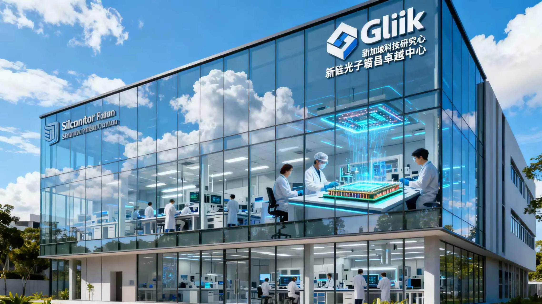
1. Target Value: AMF's 15 Years of Technological Accumulation
As the world's first professional silicon photonics foundry, AMF boasts over 15 years of industry experience. Its core competitiveness lies in three main areas: First, a mature 200mm silicon photonics manufacturing platform that can meet the needs of various scenarios such as long-distance optical communication, computing, LiDAR, and sensing; second, its self-developed process design kit (PDK), deeply optimized for telecom and data center scenarios, which can significantly shorten customers' product development cycles; and third, a complete manufacturing, prototyping, and testing service system, forming a full-chain capability from technology R&D to mass production delivery. In the acquisition announcement, GlobalFoundries CEO Tim Breen emphasized, "AMF's technological assets and talent team will perfectly complement GlobalFoundries' existing strengths." It is understood that this acquisition will fully integrate AMF's manufacturing facilities, intellectual property portfolio, and professional technical team. GlobalFoundries will leverage AMF's production capacity in Singapore to quickly fill the gap in its silicon photonics manufacturing layout in the Asia-Pacific region, forming a "dual-base" supply pattern with its existing capacity in New York, USA, and enhancing the resilience of its global supply chain. 2. Capacity Upgrade: From 200mm to 300mm Following the acquisition, GlobalFoundries will first utilize AMF's 200mm platform to meet current market demand, while simultaneously launching an upgrade plan for the 300mm platform. According to industry analysis, 300mm silicon photonics wafer manufacturing can reduce unit costs by 30%-40% and significantly increase production capacity, which is crucial for meeting the explosive growth in optical module demand from AI data centers. GlobalFoundries stated that the expansion of its 300mm platform will ensure a stable and large-scale supply of silicon photonic devices to global customers, alleviating the current supply and demand tension in the high-end optical module market. 3. Increased R&D Investment: Singapore R&D Center Focuses on 400G+ Technology To solidify its technological leadership, GlobalFoundries also announced a collaboration with the Agency for Science, Technology and Research (A*STAR) in Singapore to establish a Centre of Excellence (CoE) for silicon photonics research. The center's core R&D focus will be on next-generation materials and processes for ultra-high-speed data transmission above 400Gbps, aiming to overcome existing technological bottlenecks and further improve the transmission rate, energy efficiency, and reliability of silicon photonic devices. This R&D strategy is deeply integrated with GlobalFoundries' ten-year technology roadmap and will provide core support for the continuous iteration of pluggable optical modules and co-packaged optics (CPO). II. Core Technology: Why Silicon Photonics Has Become the "Lifeline of Computing Power" in the AI Era
1. Technological Revolution: The Debate Between Light and Electricity
The core breakthrough of silicon photonics technology lies in combining the CMOS process of traditional computing chips with optical network technology, using light pulses instead of electronic signals to transmit data. Compared with traditional copper cable connections, its advantages are revolutionary: transmission speed is increased by more than 10 times, easily achieving ultra-high-speed transmission of 400Gbps-1.6Tbps; power consumption is reduced by 3.5 times, effectively alleviating the energy consumption pressure of data centers; signal latency is significantly reduced, and anti-interference capabilities are stronger, perfectly adapting to the low-latency requirements of AI large-scale model training and inference.
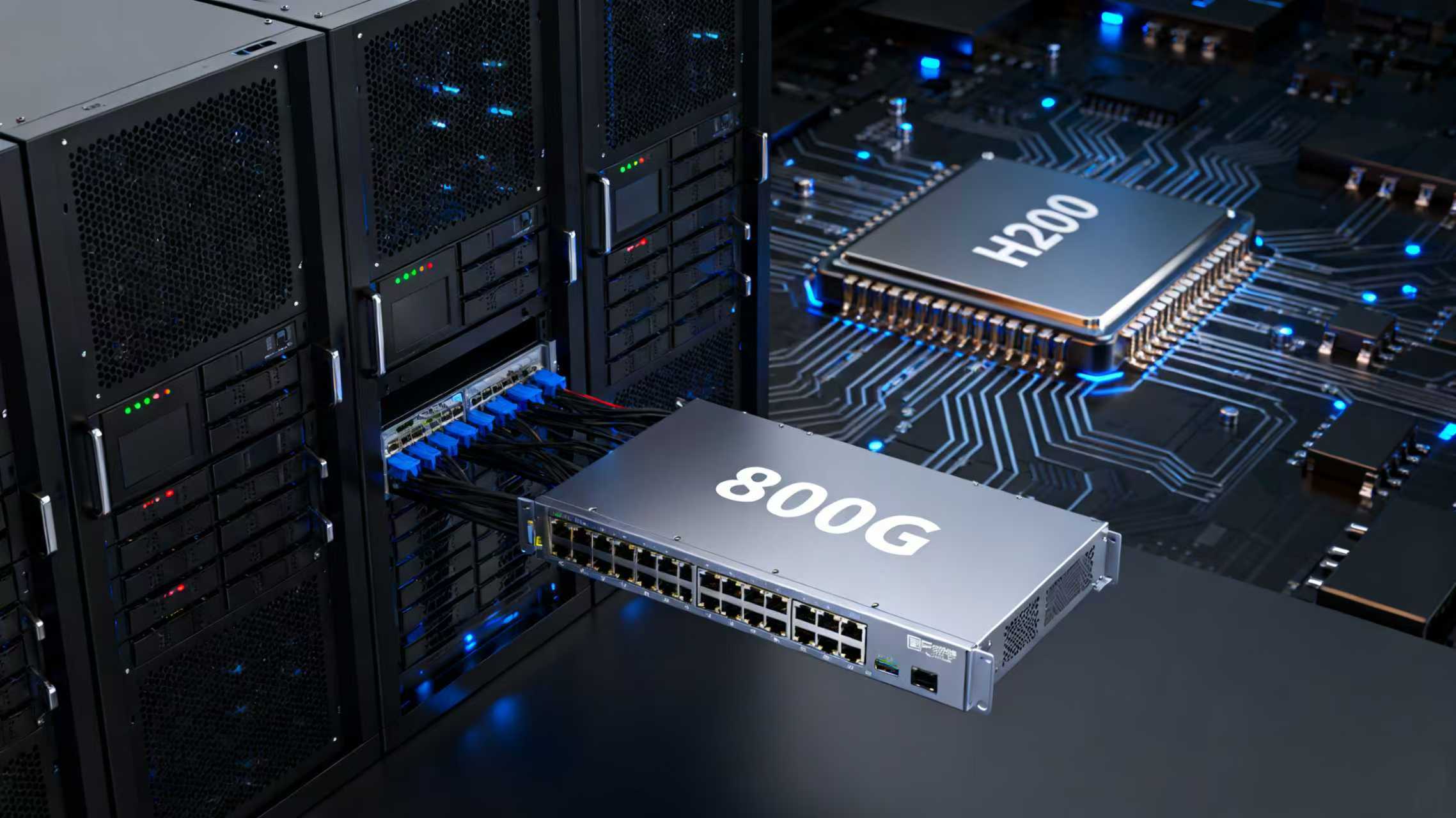
As the scale of AI large-scale model parameters exceeds trillions, the demand for data transmission bandwidth per GPU is growing exponentially. Taking NVIDIA's H200 GPU as an example, each chip requires approximately 2.5 800G optical modules to fully unleash its computing power, while the bandwidth requirements of next-generation GPUs will further increase to the 1.6T level. When traditional copper connections reach their physical limits, silicon photonics technology has become the only feasible path to break through the "computing power bottleneck." 2. Application Scenarios: Full-Scenario Coverage from Data Centers to Quantum Computing The application of silicon photonics technology is extending from core data centers to diverse fields: in the communications field, it has become the core transmission technology for 5G-A and 6G networks, supporting the needs of ultra-high-speed broadband and the industrial internet; in the automotive field, the silicon photonics-based LiDAR will significantly reduce the cost of autonomous driving sensors; in the quantum computing field, silicon photonic devices are the key carrier for realizing quantum bit interconnection. GlobalFoundries previously provided photonic chip manufacturing services to the quantum computing company PsiQuantum, and this acquisition will further strengthen its technological advantages in emerging fields. III. Market Impact: Restructuring the Industrial Chain Value and Triggering a Chain Reaction of Global Competition
1. Market Size: A Golden Track with a CAGR Exceeding 25%
The silicon photonics market is experiencing explosive growth. According to Grand View Research, the global silicon photonics market size will surge from $1.29 billion in 2022 to $8.13 billion in 2030, with a CAGR of 25.8%. A report by Ruijie Consulting shows that the global silicon photonics device market size reached RMB 27.217 billion in 2025 and is expected to exceed RMB 116.9 billion by 2032, with a CAGR of 23.15%. Specifically in the optical module field, the penetration rate of silicon photonics technology is rapidly increasing. According to LightCounting data, silicon photonics modules accounted for 30% of the global optical module market in 2025, with silicon photonics solutions accounting for as much as 50% of 800G optical modules. This proportion is projected to exceed 60% by 2030, becoming the absolute mainstream technology. GlobalFoundries' entry at this time perfectly positions it within the golden period of market growth.
2. Competitive Landscape: A Paradigm Shift from "Packaging-Driven" to "Chip Design-Driven"
For a long time, the value of the optical module industry has been concentrated in the packaging stage, with processes such as precision alignment and fiber coupling accounting for 70%-80% of the total cost. However, the rise of silicon photonics technology is shifting the core of industry competition to the chip design and manufacturing stage. The integration and performance of devices such as modulators and silicon-based waveguides are becoming key factors determining product competitiveness.
GlobalFoundries' entry will further exacerbate this trend. As a leading global semiconductor foundry, GlobalFoundries possesses standardized manufacturing processes, an IP reuse system, and multi-project wafer (MPW) services, enabling it to reduce the cost of silicon photonics chip fabrication from tens of millions to millions of dollars, significantly lowering the R&D threshold for startups. Simultaneously, it secures customer resources through ecosystem building. This "foundry-led technology ecosystem" model will profoundly impact the competitive logic of traditional optical module companies. 3. Global Competition: Strategic Layouts of Major Players Faced with the enormous potential of the silicon photonics market, global technology giants have been ramping up their investments: Nvidia launched a silicon photonics-based co-packaged optics (CPO) solution, integrating optical modules with switch chips, reducing power consumption by 3.5 times; TSMC is collaborating with multiple companies to advance silicon photonics chip manufacturing, focusing on the high-end data center market; Intel, Broadcom, and other companies are building full-industry chain capabilities through independent R&D and acquisitions. In the Chinese market, companies like InnoLight Technology and Eoptolink have deeply invested in 800G silicon photonics modules, while companies like Accelink Technologies and Tianfu Communication are transforming towards optical engine integration. GlobalFoundries' acquisition will further intensify competition in the global market, especially in the high-end 1.6T market, where the battle for technical standards and patent portfolios will become increasingly fierce.
IV. Future Outlook: GlobalFoundries' Silicon Photonics Strategy and Industry Transformation
1. GlobalFoundries' Ten-Year Roadmap: Full-Chain Penetration from Devices to Systems
In a media interview, Tim Breen revealed that GlobalFoundries' silicon photonics strategy will be divided into three phases: Short-term (1-3 years): consolidating its position as the world's largest pure silicon photonics foundry and improving its 200mm and 300mm capacity layout; Mid-term (3-5 years): expanding into integrated solutions such as co-packaged optics (CPO), deeply integrating silicon photonics technology with chip packaging; Long-term (5-10 years): promoting the extension of silicon photonics technology to adjacent markets such as automotive and quantum computing, creating a multi-scenario application ecosystem. This strategy is highly aligned with industry development trends. As data centers shift from "computing power intensive" to "bandwidth intensive," CPO technology will become the core architecture of next-generation data center networks, and GlobalFoundries, through the synergy of silicon photonics manufacturing and packaging technologies, is expected to dominate this field. 2. Value Redistribution in the Industry Chain: Who Will Control Pricing? The rise of silicon photonics technology is triggering a redistribution of value in the industry chain. A research report from Guosheng Communications points out that the value share of silicon photonics chip design has increased from 20% in traditional optical modules to over 40%, becoming the most profitable segment in the industry chain. Foundries, through process standardization and PDK ecosystem building, are gradually gaining industry influence—once a customer adopts a particular foundry's process platform, the switching cost is extremely high, creating strong customer loyalty. Analysis suggests that future pricing power in the industry chain will concentrate on integrated "design-manufacturing" companies. GlobalFoundries, through its acquisition of AMF, already possesses core capabilities from silicon photonics chip manufacturing to process toolkit provision. If it can further integrate packaging resources, it is expected to become a "rule-maker" in the global silicon photonics field. For traditional optical module companies, those unable to master core chip design capabilities will gradually be relegated to OEM/ODM assembly roles, with profit margins continuously squeezed.

3. Industry Challenges: A Dual Test of Technological Breakthrough and Cost Control
Despite its promising prospects, the large-scale application of silicon photonics technology still faces multiple challenges. From a technical perspective, integrating the indium phosphide modulator and DSP chip in a 1.6T optical module is extremely difficult, requiring sub-micron level coupling precision, and thermal management complexity increases exponentially. From a cost perspective, the initial price of a 1.6T silicon photonic module is expected to be 2-3 times that of an 800G product. How to reduce costs through large-scale production and process optimization is a common challenge for all companies.
Furthermore, the lack of unified industry standards also restricts market development. Insufficient compatibility of PDK toolkits from different companies leads to high costs for customer product development and iteration. If GlobalFoundries can collaborate with industry partners to promote PDK standardization, it will significantly lower the industry's innovation threshold and accelerate the widespread application of silicon photonics technology. Conclusion: The New Global Industrial Order in the Era of Computing Power Interconnection Behind GlobalFoundries' acquisition of AMF lies a profound shift in the competitive logic of the global semiconductor industry—when chip computing power is no longer the sole bottleneck, "how to make data run faster and more efficiently" has become the new focus of competition. Silicon photonics technology, as a "superhighway" connecting computing power and data, has strategic value no less than that of advanced process chips. This acquisition not only elevates GlobalFoundries to the top of the global silicon photonics foundry market but will also trigger a chain reaction across the global industrial chain: competition for technical standards, restructuring of supply chains, and innovation in business models will all unfold in the coming years. For AI companies and data center operators, this transformation will bring more efficient and economical optical interconnect solutions, accelerating the release of computing power; for companies across the industry chain, it requires redefining their roles, either by mastering core technologies or by cultivating niche markets, in order to establish themselves in the new industrial order. With the establishment of its R&D center in Singapore and the advancement of its 300mm production capacity, GlobalFoundries is using technology and production capacity as its two driving forces to propel the global silicon photonics industry into a new stage of large-scale development. This global race for interconnected computing power has only just begun.