


Nvidia Unveils US-Made Blackwell Wafers with 2nm Technology
Advanced process computing cores are born in the United States.
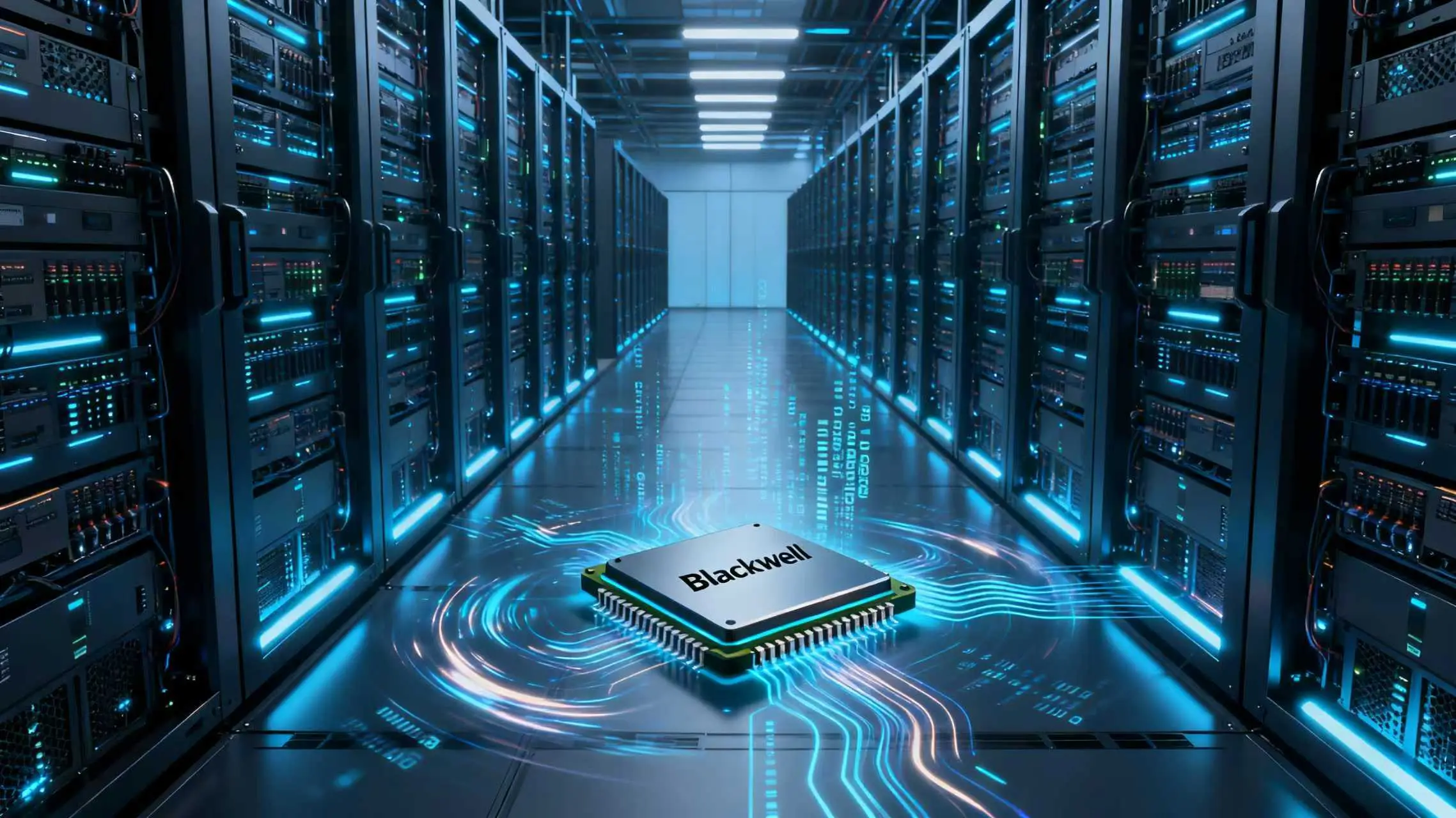
On October 18th, local time, inside the cleanroom of TSMC's Arizona Fab 21, Nvidia CEO Jensen Huang, holding a wafer emblazoned with the "Made in USA" logo, officially announced the mass production of the first Blackwell architecture chip manufactured in the United States. This chip core, which covers 2nm, 3nm, and 4nm processes, not only marks the first large-scale export of TSMC's advanced overseas production capacity but also signals that the United States has broken its long-standing reliance on Asian production capacity in high-end semiconductor manufacturing, injecting a "domestic computing engine" into next-generation communications systems and supercomputing centers.
TSMC Chairman Wei Zhejia confirmed in a concurrent online press conference that the Arizona fab has achieved stable mass production of Blackwell chips using the 4NP process, with a yield rate reaching 90%, comparable to that of domestic Taiwanese fabs. The 2nm process has also completed technical verification and entered trial production. The factory's initial monthly production capacity is planned to be 15,000 12-inch wafers, increasing to 24,000 wafers by 2026, capable of meeting 30% of global demand for high-end AI chips. U.S. Deputy Secretary of Commerce Raymond O'Rourke stated on the scene that this was a "landmark achievement" in the implementation of the Chips and Science Act, demonstrating the United States' ability to rebuild its high-end manufacturing ecosystem.
Technology Decoded: The Computing Power Revolution of the Blackwell Architecture
As Nvidia's flagship product following Hopper, the American-made Blackwell chip reshapes the technological paradigm of high-performance computing through seven major technological breakthroughs, providing critical support for next-generation communications systems:

Dual Breakthroughs in Process and Architecture
The chip utilizes TSMC's N4 and 2nm advanced process technology, integrating 208 billion transistors, 2.6 times the number of the previous generation Hopper architecture. The innovative dual-die module design enables 10TB/s inter-module interconnection via the NV-HBI high-bandwidth interface, ensuring a significant performance boost while maintaining CUDA programming model compatibility, allowing developers to seamlessly migrate applications. This architectural design easily addresses the real-time terahertz signal processing requirements of 6G communications, providing the hardware foundation for massive data analysis at base stations.
Exponential Boost in Computing Performance
The Blackwell chip, equipped with 160 stream processors and 640 fifth-generation Tensor Cores, supports the groundbreaking NVFP4 precision format, delivering 15 PetaFLOPS of computing power in intensive computing scenarios—a 7.5x increase over the Hopper architecture and a 1.5x increase over the base Blackwell chip. The SFU, designed for AI attention mechanisms, doubles throughput, reducing inference latency for large models by 50%, perfectly meeting the millisecond-level response requirements of 6G communications. Fifth-generation NVLink interconnect technology seamlessly connects 576 GPUs, achieving 130 TB/s of GPU bandwidth within a single NVL72 domain, providing distributed computing power for multi-base station collaborative communication networks.
Comprehensive Upgrades in Energy Efficiency and Security
By optimizing data reuse with 256KB Tensor Memory and combining advanced process technology, the Blackwell chip delivers three times the computing power per watt compared to its predecessor. Under typical data center loads, it can reduce server cluster energy consumption by 40%, significantly reducing operating costs for 6G base stations requiring dense deployment of computing nodes. Furthermore, its built-in confidential computing module supports TEE-I/O protection, enabling encrypted processing of sensitive communication data without compromising performance, providing hardware-level assurance for secure communications during the transition from 5G-A to 6G. Strategic Implementation: Local Manufacturing Driven by Policy and Market Forces
The Blackwell chip's transformation to "Made in the USA" is the inevitable result of the synergy between policy impetus and market demand, reflecting three core strategic principles:
The urgent need for supply chain security
"Geopolitical volatility has made supply chain resilience the bottom line for survival," Jensen Huang stated frankly in a media interview. As global semiconductor trade frictions intensify, Nvidia's previous reliance on Asian production capacity faces the dual risks of tariffs and export controls. US-based production capacity has shortened Blackwell chip delivery cycles from 16 weeks to 8 weeks, mitigating the risk of cross-regional supply chain disruptions. This deployment has reportedly helped Nvidia's H20 chip successfully pass US government export compliance reviews, avoiding inclusion on the China Control List and preserving market space for expansion in the communications equipment sector.
Precisely Seizing Policy Dividends
TSMC received $6.6 billion in direct subsidies and $5 billion in low-interest loans for the construction of its Arizona factory. Its customized production line for Nvidia also enjoys additional tax benefits. Although Nvidia did not directly receive subsidies, it indirectly reduced manufacturing costs through capacity expansion by its partners and, with the "Made in the USA" label, secured priority government procurement status. According to industry sources, Nvidia has leveraged this advantage to secure 30% of the chip orders for the US Department of Defense's 5G base station upgrade project, with a contract value of $1.2 billion.
A Rigid Response to Computing Power Demand
Global AI computing power demand is doubling every six months. Training models with hundreds of billions of parameters by giants like OpenAI requires clusters of millions of GPUs, while next-generation communication systems' beamforming and intelligent networking capabilities require distributed computing power at base stations. Production capacity from the Arizona factory will be primarily supplied to cloud providers like Microsoft Azure and Amazon AWS, as well as telecom operators like Verizon and AT&T. AWS CTO Werner Vogel revealed that the first batch of US-made Blackwell chips will be used to upgrade the Virginia Supercomputing Center, supporting the expansion of its generative AI services and the deployment of its 5G-A test network. Industry Impact: Reshaping the Communications and Computing Power Landscape
The local mass production of the Blackwell chip is like a stone dropped into a lake, sending ripples through the global fields of network equipment, semiconductor manufacturing, and communications technology.
The next-generation communications system is accelerating its implementation.
The Blackwell chip's high parallel processing capabilities provide key support for breakthroughs in 6G physical layer technology. Anna Koivisto, Vice President of R&D at Nokia Communications, stated that the chip enables real-time decoding of terahertz signals, increasing the spectrum utilization of communications systems by three times. Verizon has announced that it will deploy a trial network for the 5G-A to 6G transition, with plans to achieve commercial coverage with 10Gbps downlink speeds by 2026. Huawei, a major Chinese communications equipment giant, has also revealed that it is optimizing base station algorithms based on the computing power characteristics of the Blackwell chip to address technological competition in the global communications equipment market.
A Comprehensive Restructuring of Data Center Architecture
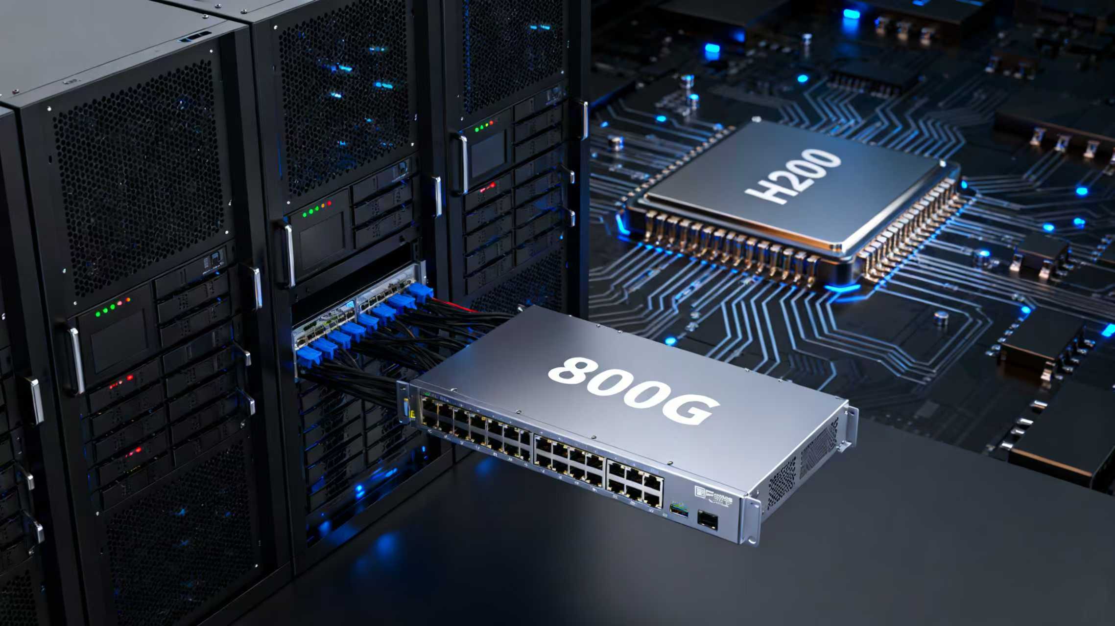
Hyperscale data centers are experiencing a wave of computing power upgrades. Google Cloud announced it will build a next-generation TPU cluster based on the US-made Blackwell chip, increasing computing power density to 10 PFLOPS per cabinet and reducing footprint by 70% compared to current systems. This leap in computing power is directly driving network equipment upgrades to higher speeds. Cisco has begun developing 800G switches, while Huawei plans to release intelligent optical modules that support Blackwell cluster interconnection, increasing transmission speeds by four times compared to existing products. TrendForce analyst Zhang Yining noted, "Each Blackwell chip will drive demand for at least $100,000 worth of network equipment."
The "Bipolar Evolution" of the Semiconductor Landscape
Previously, Asia accounted for 90% of the world's advanced process capacity. The breakthrough at the Arizona plant is breaking this monopoly. Market research firms predict that by 2028, the United States will account for 25% of global 2nm-4nm process capacity, creating a "bipolar US-Asia" landscape. However, cost pressures cannot be ignored: labor and energy costs for domestic manufacturing in the United States are two to three times higher than in Asia, leading to an expected 30% price increase for the Blackwell chip. Server manufacturers such as Dell and HP have already announced adjustments to pricing for their high-end product lines, while small and medium-sized communications equipment manufacturers face even greater cost-pass-through pressure.
Real Challenges: Triple Concerns in the Localization Process
Despite this significant milestone, US semiconductor localization still faces multiple bottlenecks, from technological breakthroughs to ecosystem maturity. These challenges will also affect the production capacity release and application of Blackwell chips:
Talent Gap Constrains Capacity Ramp-up
TSMC's Arizona plant was previously delayed due to a shortage of skilled workers, and currently faces a shortage of 2,000 engineers. Data from the Semiconductor Industry Association indicates that the United States will need 700,000 new chip industry workers over the next five years, but graduates from relevant programs at local universities can only meet 30% of the demand. To alleviate this problem, Nvidia has partnered with Arizona State University to launch a "Chip Manufacturing Specialty Program," but the first graduates will not enter the factory until 2026, potentially slowing the pace of capacity expansion in the short term. Supply chain dependence remains a challenge.
Of the 19 key materials needed for chip manufacturing, domestic production capacity in the United States accounts for less than 15%, and materials like rare earths and high-purity silicon remain dependent on imports. The recent escalation of tariff tensions between China and the United States, with China tightening rare earth export controls, has put pressure on the supply of raw materials for Blackwell chip packaging. TSMC's supply chain manager revealed that the factory's high-end photoresist is still imported from Japan, adding two weeks to the logistics cycle compared to domestic Taiwan, and supply chain resilience still needs to be strengthened.
Policy continuity is in doubt.
The Trump administration has been vacillating on the Chips and Science Act, repeatedly threatening to cut subsidies. Analysts worry that policy fluctuations could impact TSMC's subsequent $100 billion investment plan, hindering Blackwell's capacity expansion. Furthermore, differing environmental standards across US states create uncertainty for factory operations. Arizona's proposed new environmental regulations could delay the factory expansion. Multiple responses: Industry leaders interpret the impact on the industry.
"American-made Blackwell is not the end, but the beginning." At the production capacity launch conference, Jensen Huang announced that over the next four years, he will work with partners to build a $500 billion AI infrastructure in the United States, creating hundreds of thousands of jobs. He emphasized that Blackwell chips will be deeply integrated with Microsoft and Amazon's cloud services to provide computing power for edge computing nodes in 6G communications.
Huawei Consumer Business Group CEO Richard Yu stated, "Changes in the geographical distribution of advanced manufacturing processes will have short-term impacts, but technological innovation remains our core competitive advantage. Huawei will accelerate the development of its proprietary chip ecosystem to respond to changes in the industry landscape." Telecommunications equipment giants such as Ericsson and Nokia have already deployed personnel to their Arizona factory to conduct chip and base station adaptation testing. The first batch of communications equipment equipped with American-made Blackwell chips is expected to be available in early 2026.
The competition for computing power has entered a new era of "domestic manufacturing."
The birth of Nvidia's American-made Blackwell wafers is both an inevitable result of the evolution of semiconductor technology and a microcosm of global technological competition. The domestic deployment of the 2nm process not only secures a strategic advantage for the United States in the computing power race, but will also drive technological revolutions in next-generation communications, AI computing, and other fields. Its 15 PetaFLOPS of computing power and 10TB/s of interconnect bandwidth are bringing 6G communications' millisecond-level response times and trillions of connections from concept to reality.
However, challenges such as talent shortages and supply chain disruptions remind us that the semiconductor industry's global DNA is difficult to completely sever. In the future, balancing domestic security with global collaboration will become a must-do for all tech giants. For the network equipment industry, this computing revolution has already begun: 800G routers and smart base stations equipped with Blackwell chips will be mass-produced in early 2026, ushering in a qualitative leap in the transmission efficiency and intelligence of global communications networks.